
Revolutionizing the Production of Electronic Components
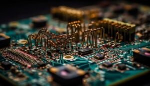
In the fast-evolving world of electronics, the development and manufacturing of printed circuit boards (PCBs) are critical to innovation. One method that has significantly enhanced the production efficiency and quality of PCBs is the use of presensitized PCBs. These boards, integral to the manufacturing of electronic components, streamline the PCB fabrication process, offering precision and convenience. This article delves into the technology, advantages, applications, and future trends of presensitized PCBs, emphasizing their role in the development of electronic components.
What is a Presensitized PCB?
A presensitized PCB is a type of printed circuit board pre-coated with a light-sensitive material, typically a photoresist. This coating allows for precise patterning of electrical traces and pads by exposing the board to ultraviolet (UV) light through a photomask. The photoresist reacts to the UV light, creating a pattern that can be developed to reveal the copper traces necessary for electronic circuits.
Composition and Structure of Presensitized PCBs
Presensitized PCBs typically consist of several layers, each contributing to the board’s functionality and performance:
- Substrate
- Material: Often made of fiberglass-reinforced epoxy laminate (FR4) or other insulating materials.
- Purpose: Provides mechanical support and electrical insulation for the copper traces and components.
- Copper Layer
- Material: A thin sheet of copper laminated onto the substrate.
- Purpose: Forms the conductive pathways for the electronic circuits.
- Photoresist Layer
- Material: A light-sensitive chemical compound.
- Purpose: Enables the precise etching of the copper layer by reacting to UV light and protecting selected areas during the development process.
- Protective Film
- Material: A removable plastic or paper cover.
- Purpose: Protects the photoresist layer from accidental exposure and damage before use.
How Presensitized PCBs Work
The fabrication process using presensitized PCBs involves several key steps:
- Design Creation
- Step: Design the circuit pattern using CAD software.
- Purpose: Create a digital layout of the circuit, defining the traces, pads, and vias.
- Photomask Preparation
- Step: Print the design onto a transparent film or use a pre-made photomask.
- Purpose: Serve as a stencil for exposing the PCB to UV light, creating the desired pattern.
- Exposure
- Step: Place the photomask over the presensitized PCB and expose it to UV light.
- Purpose: Harden the photoresist in areas exposed to UV light, leaving the rest unchanged.
- Development
- Step: Develop the exposed PCB using a developer solution to remove the unexposed photoresist.
- Purpose: Reveal the copper areas that need to be etched away, leaving the desired circuit pattern.
- Etching
- Step: Immerse the developed PCB in an etching solution to remove the exposed copper.
- Purpose: Create the final circuit pattern by dissolving the unwanted copper, leaving behind the protected traces and pads.
- Final Processing
- Step: Clean, drill, and prepare the board for component assembly.
- Purpose: Complete the PCB fabrication, readying it for mounting electronic components.
Advantages of Presensitized PCBs
Using presensitized PCBs in the production of electronic components offers several advantages:
- Precision and Accuracy
- Advantage: Provides high-resolution patterning capabilities.
- Impact: Ensures accurate and intricate circuit designs, supporting the development of complex electronic components.
- Simplified Process
- Advantage: Eliminates the need for manual photoresist application.
- Impact: Reduces preparation time and the potential for errors, streamlining the PCB fabrication process.
- Consistency and Reliability
- Advantage: Delivers consistent coating quality across boards.
- Impact: Enhances the reliability and uniformity of the final product, critical for high-performance electronic components.
- Reduced Waste
- Advantage: Minimizes excess use of photoresist and chemicals.
- Impact: Promotes environmentally friendly manufacturing practices by reducing material waste and chemical usage.
- Cost-Effectiveness
- Advantage: Lowers production costs by reducing labor and material expenses.
- Impact: Makes it economically feasible to produce PCBs in small batches or prototypes, supporting rapid development and iteration.
- Compatibility with Various Technologies
- Advantage: Supports both traditional etching and modern photolithography techniques.
- Impact: Offers flexibility in manufacturing processes, accommodating different technological needs and innovations.
Applications of Presensitized PCBs in Electronic Components
Presensitized PCBs are widely used in various applications where precise and reliable electronic connections are crucial:
- Consumer Electronics
- Application: Used in devices such as smartphones, tablets, and wearable tech.
- Benefit: Enables the production of compact and high-density PCBs, essential for modern, lightweight consumer gadgets.
- Industrial Equipment
- Application: Integrated into control systems, sensors, and automation equipment.
- Benefit: Provides robust and reliable circuitry for industrial applications, ensuring efficient and dependable operation.
- Automotive Electronics
- Application: Essential for electronic control units (ECUs), sensors, and infotainment systems in vehicles.
- Benefit: Supports the production of durable and high-performance PCBs, crucial for automotive reliability and safety.
- Medical Devices
- Application: Incorporated in diagnostic equipment, wearable health monitors, and medical instruments.
- Benefit: Facilitates the creation of precise and reliable PCBs for sensitive medical applications, enhancing patient care and device performance.
- Telecommunications
- Application: Utilized in communication devices, base stations, and networking equipment.
- Benefit: Enables high-frequency and high-speed signal transmission, essential for modern communication technologies.
- Aerospace and Defense
- Application: Used in avionics, navigation systems, and defense electronics.
- Benefit: Provides reliable and rugged circuitry capable of withstanding extreme conditions, supporting critical aerospace and defense operations.
Technological Advancements in Presensitized PCBs
Recent technological advancements have further enhanced the capabilities and applications of presensitized PCBs:
- High-Resolution Photoresists
- Advancement: Development of photoresists capable of finer resolution patterns.
- Impact: Supports the production of more intricate and densely packed PCB designs, enabling advanced miniaturization and functionality.
- Enhanced UV Exposure Techniques
- Advancement: Use of laser direct imaging (LDI) and advanced UV exposure systems.
- Impact: Improves pattern accuracy and reduces exposure times, increasing production efficiency and precision.
- Environmentally Friendly Processes
- Advancement: Introduction of eco-friendly developers and etching solutions.
- Impact: Reduces environmental impact and compliance with green manufacturing practices, promoting sustainable PCB production.
- Multi-Layer Capabilities
- Advancement: Techniques for producing multi-layer presensitized PCBs.
- Impact: Expands the complexity and functionality of PCBs, allowing for the integration of more sophisticated electronic components.
- Automated Fabrication Systems
- Advancement: Integration of automated systems for exposure, development, and etching.
- Impact: Enhances production speed and consistency, supporting high-volume manufacturing and reducing labor costs.
- Improved Material Compatibility
- Advancement: Development of photoresists compatible with a wider range of substrates.
- Impact: Provides greater flexibility in PCB design and application, accommodating various electronic component requirements.
Selecting the Right Presensitized PCB
Choosing the appropriate presensitized PCB involves considering several factors to ensure compatibility with the intended application:
- Board Material and Thickness
- Consideration: Select based on the mechanical and thermal requirements of the application.
- Impact: Ensures the PCB can handle the operational stresses and maintain performance under expected conditions.
- Photoresist Type
- Consideration: Choose between positive and negative photoresists based on the exposure and development process.
- Impact: Determines the precision and ease of the patterning process, affecting the final circuit quality.
- Exposure Requirements
- Consideration: Assess the UV exposure equipment and settings needed for the chosen photoresist.
- Impact: Ensures accurate and efficient exposure, optimizing the quality of the circuit pattern.
- Development and Etching Solutions
- Consideration: Evaluate the compatibility of development and etching solutions with the photoresist and board material.
- Impact: Facilitates effective pattern development and copper removal, achieving the desired circuit layout.
- Application-Specific Needs
- Consideration: Understand the electrical, mechanical, and environmental requirements of the application.
- Impact: Guarantees the PCB will perform reliably and meet the specific demands of the electronic components being produced.
Challenges and Future Prospects
While presensitized PCBs offer numerous benefits, they also present certain challenges that need to be addressed:
- Exposure Sensitivity
- Challenge: Ensuring consistent and precise exposure to UV light.
- Solution: Advancements in exposure technology and improved photoresist formulations are enhancing exposure reliability.
- Chemical Handling
- Challenge: Managing the safe use and disposal of chemicals used in development and etching.
- Solution: Development of safer, more environmentally friendly chemicals is reducing risks and promoting sustainable practices.
- Cost Considerations
- Challenge: Balancing the cost of high-quality presensitized PCBs with production budgets.
- Solution: Innovations in materials and manufacturing processes are helping to reduce costs while maintaining quality.
The future of presensitized PCBs looks promising, with ongoing advancements expected to further enhance their capabilities and applications. Innovations in photoresist technology, exposure systems, and multi-layer fabrication techniques are likely to drive further developments, making presensitized PCBs even more versatile and efficient in the production of electronic components.
Conclusion
Presensitized PCBs have revolutionized the production of electronic components, offering a precise, reliable, and cost-effective solution for PCB fabrication. Their advanced design and manufacturing process provide numerous advantages, including high-resolution patterning, simplified production, and environmental benefits. As technology continues to advance, presensitized PCBs are poised to play an increasingly vital role in the development of innovative electronic components, supporting a wide range of applications from consumer electronics to aerospace. For manufacturers seeking to enhance their PCB production capabilities, investing in presensitized PCBs is a strategic decision that promises significant benefits in efficiency, quality, and sustainability.


+ There are no comments
Add yours